FPGA Design Services by TronicsZone
TronicsZone is a reputed company providing professional FPGA Design services. We are well established with proven track record & in existence since 21+ years.
FPGA based design work executed by TronicsZone are known to be reliable, robust & cost effective with several of designs completed & deployed successfully.
FPGA based designs are used where critical timing is important & needs to be deterministic. They find their applications mostly in high performance defense & aerospace applications where standard microcontrollers may not be able to meet the stringent timing & performance requirements.
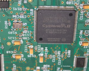
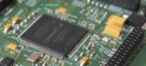
TronicsZone has experience using most popular FPGAs from both Xilinx & Altera (now Intel). We have worked on FPGA families such as Kintex-7, Artix-7, Spartan-6, Cyclone II, Cyclone III and so on. TronicsZone has experience in using FPGAs for high speed data acquisition as well as signal processing.
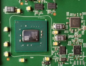
We have the capabilities for designing & testing complex boards based on FPGAs with complex BGA packages and high speed interfaces such as DDR3, high speed LVDS, USB3.0 and so on.
Our FPGA Design Examples
FPGA Design And Their Applications
The contemporary world is surrounded by various technological advancements. The lives of humans are greatly dependent on the evolving technology in every field for living satisfactory and convenient lives. Electronic devices and semiconductor chips act a primary role in developing several technological devices for the consumers as well as for the industries.
There exist several varieties of semiconductor devices and chips, which are used in the various scenarios and applications. One such innovative semiconductor device is the FPGA, i.e. Field-programmable gate arrays, which are providing new ways for the industries to develop a wide spectrum of applications since decades.

FPGA – Field Programmable Gate Array
FPGA, also known as Field-Programmable Gate Array is a semiconductor device which is used to perform logical operations. These electronic devices are an integrated set of programmable logic blocks enclosed by I/O blocks which are embedded on a chip and their internal circuits are designed with the help of programmable logic gates. They contain separate configurable logic blocks that are interconnected to the programmable connection.
With the use of semiconductor technology in the FPGA construction process, these devices have the abilities to be programmed easily when exposed to the field as compared to other categories of semiconductor chips that are not very flexible in their designing and execution process.
The reason behind the wide use of FPGAs is that they can be easily reused and reprogrammed, and are highly flexible as it can easily adapt the personalization and customization of the designer when it is placed in the field.
That is why FPGA chips highly reliable and considerable in various applications as compared to ASICs chips, which can only execute one function at a time and the program loaded on the chip, cannot be either erased or modified.
By using an FPGA chip, any program can be easily written by a person, which executes the functions after getting loaded on the silicon chip. Anyone can optimize his/her chips with the help of FPGA chips according to some workload. Aforementioned, An FPGA is a field-programmable device, so it delivers more flexibility and scalability.
These semiconductor devices can fulfill contemporary requirements of large complexity and great performance devices. Not only this, but they also deliver embedded processors, higher logic density, clocking and DSP blocks with their various prominent features.
Features in FPGA design:
Modern field-programmable gate arrays consist of a large number of RAM blocks and logic gates which are used to complicated digital computations. The design of FPGA has several bidirectional data buses and high speed I/O units, so it is difficult to verify accurate timing on proper data between setup and hold time. The feature of floor planning allows the allocation of resources within FPGAs to fulfill such time constraints.
These semiconductor devices are largely used to perform several logical functions which can be easily carried out by an ASIC as well. Certain FPGAs have analog features along with digital functions.
A typical analog feature is the programmable slew rate which is implemented on every output pin, which permits the designer to set the lightly loaded pins on low rates to prevent the unacceptable occurrence of coupling or ring, and set the heavily loaded pins on high rates when deployed on fast-moving channels, otherwise, it would work extremely slowly.
Various common features like RC oscillators, phase-locked loop implemented with voltage-controlled oscillators and quartz-crystal oscillators, which are implied in the management and clock generation for rapid serializer-deserializer to transmit clocks and its recovery clock time.
Various differential comparators are positioned at the input pins to connect differential signalling channels. FPGAs also have completely outlined analog-to-digital converters & vice-versa along with signal conditioning units which permit them to function as SOCs.
Different types of FPGA design:
The design architecture of the FPGA is widely responsible for its performance and density. FPGAs can be constructed into different designs depending on various parameters. Following is the list of different types of FPGA design:
On the basis of the internal alignment of logic blocks, FPGAs are divided into three types:
- Symmetrical arrays
In this type of arrangement, the logic blocks are aligned in the form of the matrix, consisting of rows and columns and other interconnect components arranged between them. The I/O blocks surround this symmetrical matrix which can be connected to the external devices.
- Row-based architecture
In this type of architecture, the rows of programmable interconnect tracks are alternated with the rows of the logic blocks and the I/O blocks are positioned at the edge of each row. A single row may form connections with the adjacent rows through vertical interconnect.
- Hierarchical PLDs
In this type of arrangement, FPGA architecture is constructed in a hierarchical manner in which the highest level contains only interconnects and logic blocks. Every logic block consists of numerous logic modules and every logic module contains sequential as well as combinational functional elements.
On the basis of the FPGAs programming technologies, they can be classified into three categories:
- SRAM-based FPGAs
These types of FPGAs contain Static RAM cells, which can control transmission gates, multiplexers or pass-transistor. These semiconductor devices are re-programmable with its upgraded designs, however, if the power is disconnected, the whole programming will be lost which requires to be configured when starting it. Hence, external memory is required by these devices to keep the program safe.
- Antifuse-based FPGAs
Such FPGAs utilize antifuse CMOS technology for programming them. Once an engineer completes programming the FPGA, then it is not possible to reprogram it. These devices can keep their program even if the power is switched off.
- Flash-based FPGAs
These kinds of FPGAs utilize floating gate cells in the form of switches to enhance area efficiency. Such FPGAs are not prone to lose information even when the power supply is disconnected. Moreover, they do not require external memory to keep the program; however, they are unable to reprogram themselves for an infinite number of times because charge gets buildup inside oxide.
On the basis of the application’s usage, FPGAs can be categorized into three types which are described below:
- Low-End FPGAs: These types of FPGAs are the most suitable for those systems which require logic density, low complexity and low power consumption of the chip.
- Mid-Range FPGAs: These kinds of FPGAs are regarded to provide the ideal solutions in many applications as it maintains a balance between density, consumption and complexity on a single chip within the cost range without needing to compromise in a large extend on either price or performance factor.
- High-End FPGAs: These types of semiconductor devices are highly expensive and consume high power compared to their other types. But keeping these factors, these devices provide the best kind of functionality with maximum complexity and logic density, along with the best device performance.
Various applications of FPGAs:
FPGAs deliver manifold advantageous features which, when taken into consideration can be useful to develop varied types of applications. Since these semiconductor devices are commonly used for high complexity and low volume projects as they deliver higher customization power. Following is the detailed description of the latest applications used in various industries:
- The introduction of FPGA chips in business has opened up several new ways for secure technology and automation, which can aid several factory runners and business owners to tackle security threats and other relatable risks by enabling the automated devices in the workplace.
- FPGAs are widely used in vehicles and automotive industries which allow the use of several applications like LiDAR, Automatic Radar systems and automatic driving vehicles.
- FPGAs are largely used in the defense department to enhance security and develop automated weapons as they can easily fulfill the reliability, performance, and life-cycle requirements of serious environmental conditions, which also delivers higher flexibility as compared to the traditional feasible ASIC implementations.
- FPGAs can be utilized in analog industries to carry out different tasks of data-conversion. These devices contain analog-to-digital converters which are used to check several different signals, as well as on-chip temperature. Since FPGAs delivers 12-bit resolution, they can convert various analog quantities into digital data for data transmission, computing, control systems and information processing. Moreover, FPGA consists of large internal memory and with numerous multipliers, so it can be used as an analog signal and digital signal processing systems. FPGA logic blocks are widely used in video and image processing applications.
- These semiconductor devices are also being used in a wide spectrum of different fields like in developing computer hardware, radio devices and medical equipment. FPGAs are also being used in the field of voice recognition technology, Bioinformatics, wired/wireless communications systems, security systems and other medical, electronics and scientific industries.
- Extensive and frequent use of FPGAs in communication systems helps to improve network coverage, network capacity along with the quality of service; which also simultaneously helps to reduce delays and latency issues, when dealing with data manipulation. Various companies are utilizing FPGAs for cloud or server applications.
- FPGAs can also be used for ASIC verification and emulation. Several interconnected FPGAs can together simulate ASIC and then enable engineers to carry out the testing and verification process before the production of ASIC chips.
- FPGAs are greatly used for developing algorithms and hardware; therefore, they are being widely used for accelerating machine learning or artificial neural network applications.


