Thermal Management Techniques in PCB design
NOTE: This article/blog is Copyright TronicsZone. It cannot be reproduced without prior written approval.
Thermal Management Techniques in PCB design
Introduction
Printed circuit boards (PCB) are the fundamental component of an electronic system. PCB’s performance enhances the performance of the entire device. With miniaturization of devices, the heat generated per unit area has increased. This, in turn, will make the components within the device to malfunction, reducing the lifetime of the device. The major heat-generating components in an electronic device are microprocessors, transistors, resistors, batteries, solder joints, and copper traces. When millions of such components are packed together within a small area, the heat level generated will increase exponentially. Excess heat included issues can be moderated by maintaining a strict thermal design procedure and providing circuit cooling facilities within the device.

Need for thermal management in PCB’s
The performance of a PCB is evaluated by its parameters such as speed, accuracy, and lifetime. Excess heat generated in a circuit will affect the performance of the circuit. Heat is generated in a PCB due to the flow of current. The heat generated in a circuit is given by
Heat Generated = I2R
Where I is the current flowing in the circuit and R is the circuit thermal resistance.
The thermal resistance is also denoted as ϴ . Value of ϴ is
ϴ = l/A * K
Where
- is the length of the thermal path
- A is the cross-sectional area of the path, and
- K is the thermal conductivity
The design goal of the engineer will be to reduce the thermal resistance of the circuit by optimizing any of these parameters to achieve better performance. Devices operating at high frequency may experience heat due to self-coupling, mutual coupling also.
The reduction of heat generation can be achieved by the component selection, placement, and orientation. Especially for high speed, high-performance applications heat management becomes essential, taking high frequency of operation and device compactness into consideration.
Analysis of Thermal profile of PCB
Thermal analysis of PCB can be done at the simulation stage or during the device test stage. The analysis provides design engineers an idea of the heat formation and transfer within the PCB. They can then use the results and simulations to come up with techniques that will help them manage the heat better. Some of the analysis techniques used are:
Visual inspection
Visually inspecting the device during operation, to find any sign of burning, overheating or damaged components. Component discoloration and burnt smell are some signs of device malfunction. Simple issues like short circuits can be identified and corrected.
Infrared camera test
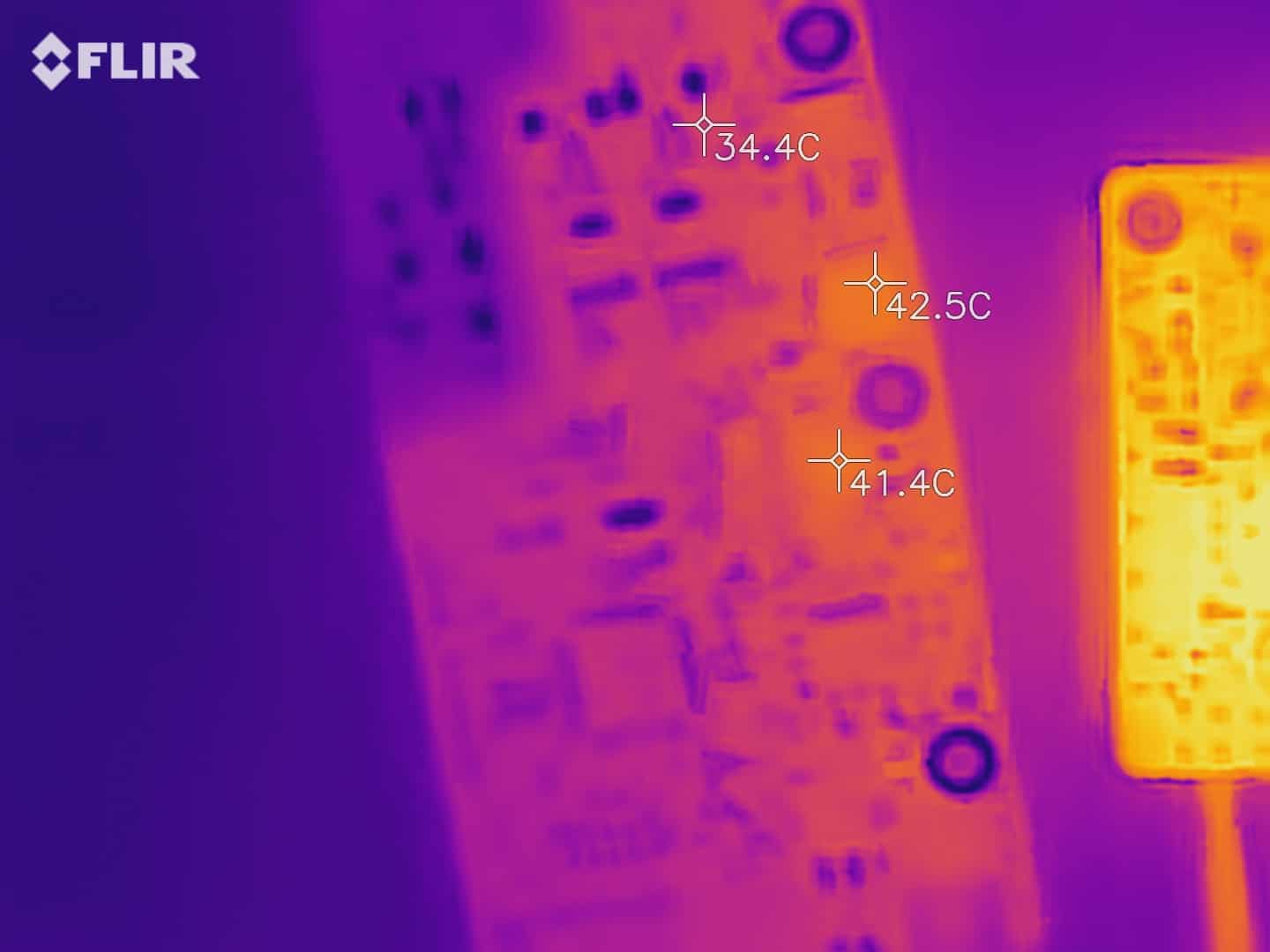
Heat vision IR cameras can pinpoint the location of heat leakage. IR analysis is useful to find counterfeit or defective components. Tracks that have insufficient solder, have higher resistance and more heat dissipation, these tracks can be identified using IR analysis.
Heat analyzer test
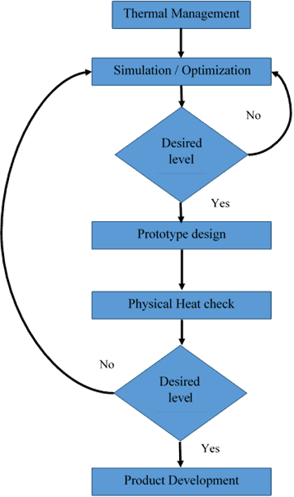
This is a pre-prototype simulation level check-up. Software simulations can report potential heat-generating areas in the design. Using this report design adjustments can be made while physically producing the PCB. Simulation largely cuts out time and cost. Simulation can also provide data on device performance in different ambient temperatures. This will enhance the reliability of the device

Figure 1: Flowchart: Steps in thermal management of PCB
PCB design techniques to dissipate heat
Design techniques and component selection can help reduce heat generation in a PCB. The common techniques include heat vias, heat sinks, heat pipes, and copper ground plate and so forth. Cooling fans are also provided in some devices to induce external cooling. A combination of two are more techniques are also employed in some devices such as a laptop where a heat sink, heat pipe, and a fan are all used.
Metal as a thermal pad
Copper is a good conductor of heat. Thick copper pads are used under a PCB as a heat dissipation pad. This technique is termed as an external heat sink. Copper plates distribute the heat all over the board thus reducing any particular component damage.
Selection of PCB materials
Designers choose PCB materials that have properties such as, stable dielectric properties over a wide range of temperature and relative humidity, consistent thermal-mechanical performance over a large temperature range, and thermal compatibility with other materials that make up the PCB. Thermally-robust PCB materials mitigate the risk of temperature changes.
Internal Heat Sink/Thermal via array design
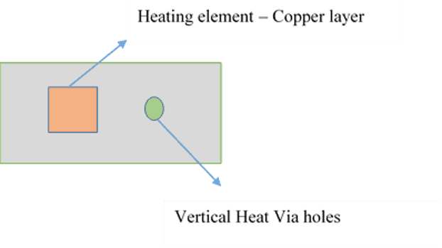
Internal heat sinks are metallic vias that conduct heat from top layers through insulating layers to distribute the heat on the copper plane embedded below. Heat via can be simple and hollow or filled with epoxy and plated with copper. Vias improve heat conduction. Thermal via reduce the thermal resistance significantly. Closer the vias are to the heat source better the conduction and better the thermal performance of the system.

Figure 2: Via design in PCB
Cooling system
Cooling system can be integrated with the device to improve heat dissipation. The Colling system can be of forced air cooling type or fluid cooling type. Forced air cooling is done by strategically placing a cooling fan to vent out the heat. Fluid cooling is done by the heat exchanger process. For compact low power devices fan is preferred, while for high heat generating critical devices fluid cooling is preferred.
Challenges in optimized thermal design
- Miniaturization of PCB area
- Circuit performance and speed
- Cost to performance ratio
- Immunity to ambient temperature
Conclusion
Designing a PCB with proper thermal management techniques ensures the robustness and reliability of the PCB. Pre-production simulation is an effective way to optimize heat dissipation. Further using external heat sinks (copper plate) and internal sinks (via) stands effective in heat management. All these methods help to make the PCB more immune to thermal issues and improves the performance and the lifetime of the product.
TronicsZone
At TronicsZone we provide reliable and customized PCB design for all your industrial needs and domestic needs. Specializing in low-cost superior quality design since 2003, we are providing quality services in Electronic product design, software development, Prototyping & Manufacturing according to custom specifications.
NOTE: This article/blog is Copyright TronicsZone. It cannot be reproduced without prior written approval.


 TronicsZone