High Speed PCB Design Techniques
NOTE: This article/blog is Copyright TronicsZone. It cannot be reproduced without prior written approval.
1. Introduction
The need for high-speed digital circuits is increasing every year, and also the demand for reliable high-speed PCB. The digital PCB circuits are compactly packed with microprocessors, power supply and many other components that are operating at frequencies easily over 1 GHz. These systems are capable of managing billions and billions of operations every second.
The performance of this setup relies on the effort made during the design stage to optimize any issues that may arise due to high-speed operation. Typical problems in high-speed PCB systems include impedance discontinuities, signal reflection, EMI, and noise generation. This article focus on such problems and the techniques to follow during PCB design to avoid them.

2. Application of High Speed PCB’s
High-speed PCB is the heart of computational devices such as computers, smartphones, and many more. These devices are complex in nature. Hence the PCB is expected to be robust and reliable. Applications of high-speed circuits are growing in the fields of communications, aerospace, and IoT. With the criticality of the application in mind, it is essential to understand the considerations that are needed to be followed while designing board layouts for high-speed circuits. Typical high-speed systems have technologies like HDMI, PCI Express, USB, or SATA incorporated. With these technologies, the designer will be dealing with high-speed design constraints.
3. Design considerations
The following are considered as the go-to techniques in designing High-speed PCB’s to achieve high speed operation in a low-power environment.
- Clock selection and optimization
- Minimizing on-board noise from the power network
- Minimizing cross-talk between signal traces
- Reducing signal reflection
- Optimizing the system for EMI form environment and self-coupling
- Proper impedance matching and line termination
- Floor planning – packaging all the components
4. Board Material selection
Selection of board material depends on the dielectric constant and loss tangent of the material. Loss tangent is the energy lost from the material when an electromagnetic wave passes through it. Higher the loss tangent, the more the energy lost. Dielectric constant of a material is given by
εr = ε/ε0
Where εr is the dielectric constant, εo is the permittivity of free space in (Farad/m) and ε is the material permittivity in (Farad/m). εo value is approximately 8.85 x 10⁻¹² farad per meter (F/m). The dielectric constant decides the impedance offered by the material and signals can propagate faster in materials that have a lower permitivity. The typical dielectric material used in PCB design is FR4. It has a permittivity value between 4.1 and 4.5 and a loss tangent value of 0.019 @ 1MHz.
4.1. Microstrip Design
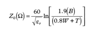
Signal trace on a single ground planes behaves like a microstip line layout and signal trace in between two ground plane acts as a stripline layout. The characteristic impedance of microstrip line is given by


Figure 1: Microstrip line
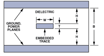
Characteristic impedance of Stripline is given by


Figure 2: Stripline controlled impedance line
To obtain same impedance values the dielectric span must be greater in stripline layouts compared with microstrip layouts, hence stripline tends to be thicker than microstrip layout.
4.2. Ground plane design
Ground planes in a PCB helps in shielding, heat dissipation, common reference voltage and reducing stray capacitance. Current in a circuit tends to low in a low impedance path. At very high frequencies fast raising signal edges are coupled to the ground plane, creating a current spike in the ground plane. This current spike damages the analog performance of the PCB. Further high-speed op-amps are affected by the presence of ground plane below as the input stray capacitance increases. To avoid these conditions proper distance is maintained between the digital devices, analog devices and the ground plane. Less-susceptible plating metals can be used as a ground plane.
5. Power supply and clock design
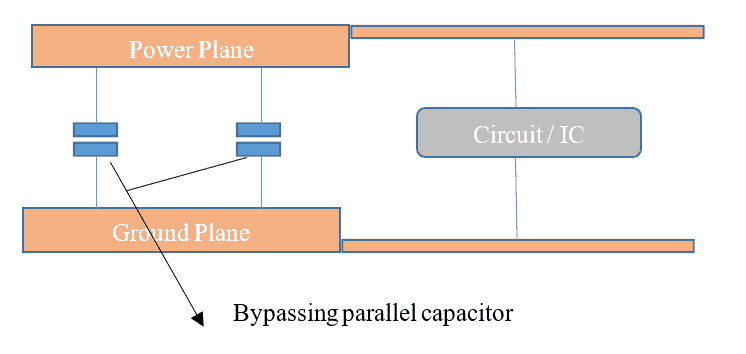
Power supply is the premium source of on-board low frequency noise in the PCB circuit. Power integrity in a high speed system can be ensured by connecting the power plane to ground plane by using parallel capacitors. Parallel capacitors of different value ensures low ac impedance across a wide band of frequencies. Separate power planes shall be used for digital and analog devices to minimize noise coupling.

Figure 3: Power supply bypassing
Clock selection is important to ensure that all signals on the PCB layout are arriving at the proper time in relation to the clock signal. Improper clock may result in raising edge detection or falling edge detection issues. This will lead to corruption of data. Speed of the clock determines the speed of the entire system.
6. Floor planning
Floor planning and packing have a significant impact on noise, communication delay, edge rate and frequency response by means of parasitic inductance, parasitic resistance and parasitic capacitance passing through the connecting lines and lead. Silicon design, packaging design and board-level design should be done along with the schematic design. Software simulations can be used to floor plan the circuit prior to physical deployment. Specifying the component locations and signal routing from the beginning itself, helps the designer to ensure that the design will work in the intended way. This lowers cost and rework time and thus reducing the cycle time of the product.
7. Signal Integrity
PCB consists of variety of signals of varying frequency, both analog and digital. These signals are sensitive to noise and coupling. Proper care in routing, shielding and impedance matching has to be taken to ensure signal integrity.
7.1. Routing
Certain guidelines to followed during routing are listed below
- The high frequency clock traces as routed as straight as possible. In case of need for bends, arc bends are preferred than right angled bend to avoid signal loss due to discontinuity.
- Terminate clock signals, this will help in minimizing reflection.
- Signal traces that are sensitive require high isolation, so they should be routed on separate layers.
- Long parallel run of striplines are reduced in close proximity of signal traces on the same board. This will reduce inductive coupling.
- Multiple via are avoided, because they can cause impedance mismatch and increase inductance.
7.2. Impedance matching
Impedance matching between the transmitter and receiver will have a direct impact on the integrity of signals. Improperly matched lines produce signal reflection and signal loss. The impedance of the source (ZS) must equal the impedance of the trace (Zo), as well as the impedance of the load (ZL). Proper termination of a transmission line ensures matching and signal integrity.
8. EMI optimization
EMI that affects a device can be due to self-coupling or mutually coupled from the other electronic devices in the surroundings. EMI can be optimized in high speed circuits using certain techniques.
8.1. Matching and routing
Unmatched or unterminated signal traces induce reflection. This causes signal ringing back to the source. This is a type of self EMI. Proper matching ensures removal of signal ringing. Proper routing also reduces self-coupled EMI.
8.2. EMI filter and shielding
Shielding in a PCB is done using an elongated ground plane. Skin effect on the conductive surface of the ground plane reduces external EMI that causes signal disturbance in the circuit. EMI filter are implemented to filter out ambient EMI noise and couple it to the ground. A simple decoupling capacitor setup can be used as an EMI filter.
9. Conclusion
In High speed PCB design it is imperative to plan everything before starting the physical layout process. A good schematic is the foundation for a good layout. Factors such as power supply location, routing, signal integrity, impedance matching are the important considerations to be addressed during the PCB design. Efficient design and implementation will enhance the reliability and robustness of the PCB.
TronicsZone
TronicsZone is a trusted expert in electronic design, building robust and reliable products since 2003. Designing cost effective, reliable PCB is an area of expertise in TronicsZone. We also provide a wide array of Electronic Design Services that includes, Custom Electronics Design, PCB Design, IoT Hardware, Firmware development, Embedded Systems Design, Prototyping & Electronic Manufacturing Services.
NOTE: This article/blog is Copyright TronicsZone. It cannot be reproduced without prior written approval.

 TronicsZone
 TronicsZone