How can Electromagnetic Compatibility (EMC) improve the quality of an Electronic device?
NOTE: This article/blog is Copyright TronicsZone. It cannot be reproduced without prior written approval.

Wireless communication technology has taken over the communication engineering arena in this last decade. With ever-increasing high-frequency signals around us, it becomes exponentially important to design every sort of electronic device to withstand all the unwanted interference and perform as expected. State of the art IoT sensors are designed to work as a network of sensors coupled with a processor or cloud server working in tandem to produce the desired results. In such a closely packed wireless network, it is essential to check and ensure the compatibility of the devices and sensors.
Electronic devices of high importance such as medical devices are the most prone to electromagnetic interference, at the same time they are the one that needs to work with high precision. Hence, designing the devices to withstand EMI and pre-delivery EMC checks are becoming an integral process in electronic manufacturing.
What is EMI?
EMI is the abbreviation for Electromagnetic interference. Every electronic device under operation emits electromagnetic waves intentionally and unintentionally. EM waves thus emitted interfere with adjacent devices or with the environment of the original device. This interaction/interference is termed as electromagnetic interference. Electronic devices may malfunction under such strong RF fields. Designing circuits accordingly with proper precautionary measures is a part of the designer schedule.
Types of EMI
Electromagnetic interference can be categorized based on the following factors
1. Source of EMI
EMI on the basis of source is of two types. Natural and man-made. Cosmic ray is a classic example of natural EMI. Solar wind causing interference on devices in the polar region is a recent area of research. Man-made sources include communication devices, radars and many more.
2. Frequency bandwidth
On the basis of frequency bandwidth there are two types. Narrowband and Broadband. Narrowband EMI is commonly intentional radiation such as tv stations, wireless communication devices. Single-frequency oscillators within these electronic devices is the source for narrowband radiation
Broadband EMI is unintentional for example radiations from power grid line, low frequency but causes a strong interference. Faulty motor brushes fluorescent lamps are some other examples.
EMI Coupling Mechanisms
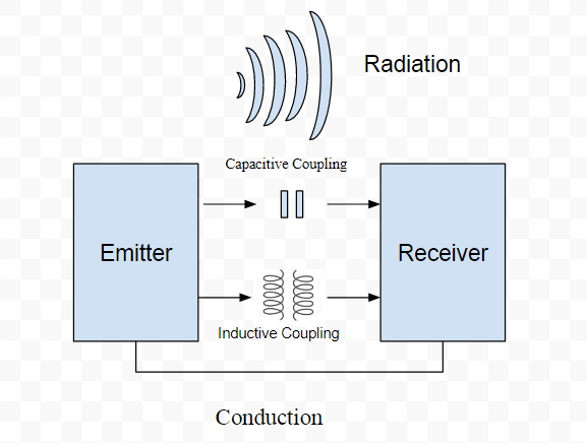
Electromagnetic waves are coupled from the source to the receiver via three mechanisms.
They are radiation, conduction and coupling (Capacitive coupling and Inductive coupling). The diagram below illustrates all three types of coupling.

Conduction occurs through a physical connection such as a common ground. Radiation occurs due to the proximity of frequency source and the receiver. Inductive coupling is due to the phenomenon of electromagnetic induction and capacitive coupling is due to charge coupling between circuit components during voltage variation.
Hazards of EMI on Electronic devices
High and continuous exposure to EMI causes damage to circuits. Devices behave abnormally and give out undesirable output. This is a critical problem especially in medical electronic devices. Consider an electronic pacemaker, any interference and subsequent faulty operation may cause fatal damage. Hence designing circuits to both withstand EMI and to emit less EMI is important.
Devices operating with modulation, demodulation circuits are the worst affected since interference noise corrupts the original signal. Spread spectrum. Frequency hopping are some techniques that can be utilized to minimize errors in such devices.
Steps to minimize EMI in PCB designs
1.Ground Plane
The ground plane of PCB acts as the first line of defence against EMI. Steps to be followed during ground plane design are
- Using multi-layer boards
- Using split ground planes
- Using decoupling capacitors to ground circuits.
2. Signal traces
- Avoiding sharp edges in signal traces. They absorb radiation
- Impedance matching at input and output
- Keeping return paths as short as possible
- Separating high-frequency signals and low-frequency signals to avoid inductance interference
3. EMI Shielding
Metal shields such as a faraday cage shall be used to protect PCB. Further, metal surfaces shall act both as ground planes and EMI shield. EM waves incident on metal planes is conducted as current only on the surface of the plane due to skin effect. This protects the inner circuits from interference. Boxes made of conductive foam or metal gaskets can also be utilized for this purpose.
Electromagnetic Compatibility
Electromagnetic compatibility or EMC is the ability of a device to function precisely with limiting its unintentional emission of electromagnetic noise and neutralize the reception of EMI from other sources around it. Three main clauses in Electromagnetic compatibility are Emission, Susceptibility, and Immunity
Emission: Tendency of the device under test to generate electromagnetic energy intentionally or unintentionally
Susceptibility: This is the tendency of a device to malfunction under EMI. Higher the susceptibility higher the damage the device suffers when unwanted signals interfere with it.
Immunity: immunity is the ability of the device to withstand any EMI and work properly. This is opposite of susceptibility
International and National standards and laws
International standards for EMC compliance include International Electrotechnical Commission (IEC), International Special Committee on Radio Interference (CISPR) and International organization for Standardisation (ISO). Different types of equipment have different standards and specifications. In India there is no regulation on EMC compliance but standardization, testing, and quality certification steps are followed to meet international standards such as IEC, ISO and US standards such as FCC (Federal Communications Commission)
EMI/EMC testing and Certification
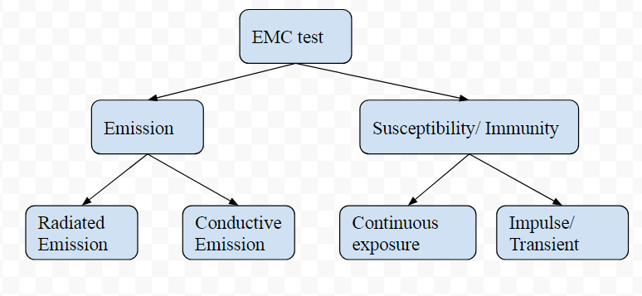
EMI/EMC testing involves measuring emission from the device under test and also measure the susceptibility of the device under test.

Typically the device under test is placed in an anechoic chamber to cut out external interference during test procedure. Radiated emission tests are done using antenna setup connected to a spectrum analyzer to measure radiation. Conduction emission test is performed using an EMI receiver via an ISN (impedance stabilization network) located within the test chamber.
Susceptibility or Immunity test is performed by placing the device under test through a continuous or impulsive EMI source to check its functionality. This testing ensures that a product works fine in a simulated RF proximity that may occur in the real world. Pre compliance testing softwares are also available to avoid device failure after physical manufacturing.
After testing certification is given in India by NABL (National Accreditation Board for Testing and Calibration Laboratories) accredited laboratories. Further, Indian labs are accredited also by international standard organizations such as TÜV Rheinland, TÜV SÜD, Det Norske Veritas (DNV), EMITECH France, Intertek, Canadian Standards Association (CSA).
Conclusion
Electromagnetic interference is an unavoidable problem in the current wireless scenario and hence considerable research has been put in to improve Electromagnetic compatibility of the devices that we design. By following standardization, testing, and quality steps as specified, EMC compliance of a device can be improved and enhance its reliability and life.
TronicsZone
At TronicsZone we provide reliable and robust Electronic Design Services. We specialize in designing electronic products that are low cost to manufacture but are superior and long lasting. We have enough experience to ensure that the products we design comply with popular EMI/EMC standards and can pass the EMI/EMC tests easily or with very little modifications.
NOTE: This article/blog is Copyright TronicsZone. It cannot be reproduced without prior written approval.

 TronicsZone