Need for Signal Conditioning in IoT Sensors
NOTE: This article/blog is Copyright TronicsZone. It cannot be reproduced without prior written approval.
Introduction
Modern sensor wireless communication devices are digital in nature, but the inter-communication between them is done via analog signals. For example in an IoT sensor setup, the communication between a sensor and the central processor is wireless and it is usually done through Wi-Fi. Wi-Fi or WLAN (IEEE 802.11) communicates in various frequencies, including but not limited to 2.4 GHz, 5 GHz, and 60 GHz frequency bands.
In cases like these at the receiver end it is essential to condition the input analog signal. Signal conditioning ensures proper retrieval of data, by efficient conversion of analog signal into digital data. Signal conditioner is an essential component of a system that interfaces with a sensor.
What is Signal Conditioning?
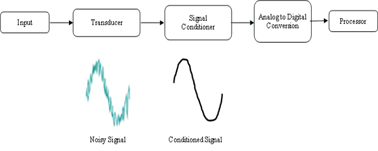
Signal conditioning is a part of data acquisition process that involves stages three important stages that are filtering, amplification and isolation. These steps are followed to make sure that the input signal is compatible with the data acquisition hardware. At TronicsZone, we firmly believe that proper designing of the signal-conditioning module is critical for maximizing the precision of the data acquisition system. The steps in signal conditioning and data acquisition are listed below.
- Amplification
- Linearization and Cold junction compensation
- Filtering
- Sampling and Digital conversion
- Isolation
- Data Acquisition

Figure 1: Digital system data acquisition
Steps in signal conditioning
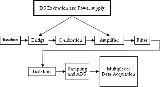
The input from transducer contains all the required data. This signal is very low in power, distorted with noise. It is important to amplify the signal initially to start the conditioning process. Amplification is preceded by calibration of the signal.
1. Amplification
Amplification is done to increase the voltage of the incoming signal. Typical voltage range for the data acquisition hardware will be 0 to (+ or -) 10V. If the signal is lower than this range it is amplified. For example a thermocouple output is in the range of millivolts. This signal is amplified to reach a value between 0 to (+ or -) 10V. If the input voltage is greater than this range voltage divider resistance network is used to divide the signal.

Figure 2: Signal Conditioning Circuit Block Diagram
Prior to amplification analog signal calibration is done. This calibration minimizes input offset, gain and nonlinearity errors introduced in the signal from the sensor prior to being digitized. A amplifier is selected based parameters such as very high open-loop gain, very high common-mode rejection ratio very low DC offset, low drift, low noise, , and very high input impedances.
2. Linearization and Cold Junction Compensation
Linearization is required when the signals produced by a sensor do not have a proportionally direct relationship with the physical measurement. For example a thermocouple output is not linear. In this case a microprocessor is used to detect the temperature in a look-up table of voltage vs temperature.
Cold junction compensation is required in case of thermal sensors such as thermocouple. In thermocouple if there is a change in temperature between two junctions an electromotive force (emf) is setup. So the emf is equivalent to the difference in temperature data only. To find the actual temperature, the cold junction temperature is added with the sensor output temperature. This is termed as cold junction compensation.
3. Filtering
After amplification and linearization stage of signal conditioning, signal must be filtered and optimized for the analog and digital converter (ADC) to read it. Filtering reduces noise errors in the signal. Typically for most of the applications a low-pass filter is used for filtering. This allows the lower frequency components to pass through but attenuates the higher frequencies. Typical sensor outputs are slowly varying hence their produce low frequency signals. So low pass filters are used. In some special cases anti-aliasing filters are used. An anti-aliasing filter is a low pass filter that restricts the output bandwidth below the Nyquist–Shannon sampling rate. This filter is typically used before the sampler module. Ideal anti-aliasing filter passes all the input frequencies (below f1) and cuts off all the undesired frequencies (above f1), where f1 is the cut-off or the Nyquist frequency.
4. Sampling – Analog to Digital Conversion
An ADC converts an analog signal to a discrete-time and discrete-amplitude digital signal. Sampling rate determines the bandwidth of the digital signal produced by the ADC. Steps in ADC conversion are
- Anti-aliasing filter
- Sampling
- Quantization
- Quantized output is digitally coded
Performance of an ADC is measured by using parameters such as signal to noise ratio (SNR) and bandwidth. The digital output is provided to the data acquisition module to retrieve the original data.
5. Isolation
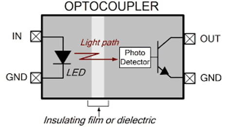
Now after sampling the analog signal is converted into a digital signal and will be further processed by digital devices. Electrical signal containing a high-voltage component will damage the digital components. A high transient voltage at one input will damage not only the input circuit, but an also can propagate to other equipment connected to that input or the device. Thus, the sensor signals should be electrically isolated from the data acquisition module to ensure protection from serious overvoltage. Optocouplers and digital isolators using silicon-dioxide dielectric capacitors can be used to provide isolation.

Figure 3: Optocoupler for Isolation
Why Signal conditioning pays off in a digital design
Signal conditioning circuit provide
- Protect signal circuits against high-frequency coupling
- Minimize radio frequency interference and electromagnetic interference.
- Signal conditioners protect digital equipment from high voltage surges through isolation
- Signal conditioners can provide reliable signal splitting, when signals are needed for several parallel processing
- Improve the accuracy of data retrieved in the digital part of the device.
Conclusion
Signal conditioning is thus an integral part of devices with analog input and digital processing unit. Most sensors require a signal conditioning circuit designed to process their input into a linear voltage that can be measured by a digital data acquisition circuit. Low power input shall be amplified and filtered to weed out noise and thus signal conditioning systems effectively increase the accuracy of data estimated.
NOTE: This article/blog is Copyright TronicsZone. It cannot be reproduced without prior written approval.

 TronicsZone
 TronicsZone